Executive Summary Cholesteatoma Market :
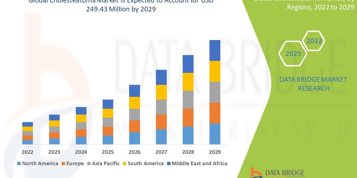
Global cholesteatoma market size was valued at USD 214.02 million in 2024 and is projected to reach USD 273.44 million by 2032, with a CAGR of 3.11% during the forecast period of 2025 to 2032.
The research and analysis carried out in this Cholesteatoma Market report helps clients to predict investment in an emerging market, expansion of market share or success of a new product with the help of global market research analysis. This market report is also enriched with historic data, present market trends, market environment, technological innovation, upcoming technologies and the technical progress in the related industry. By utilizing few steps or a number of steps, the process of formulating this Cholesteatoma Market research report is started with the expert advice. This Cholesteatoma Market research report offers the best and professional in-depth study on the existing state for the industry.
With the specific and high-tech information provided in this report, businesses can get idea about the types of consumers, consumer’s demands and preferences, their perspectives regarding the product, their buying intentions, their response to particular product, and their varying tastes about the specific product which is already present in the market. All the statistical and numerical data that has been estimated in this Cholesteatoma Market report is represented with the help of graphs, charts, or tables which makes this report more user friendly. Complete compilation of company profiles that are driving the market is also performed in this report.
Discover the latest trends, growth opportunities, and strategic insights in our comprehensive Cholesteatoma Market report. Download Full Report: https://www.databridgemarketresearch.com/reports/global-cholesteatoma-market
Cholesteatoma Market Overview
**Segments**
- By Type: Congenital Cholesteatoma, Acquired Cholesteatoma
- By Treatment: Medications, Surgery
- By End-User: Hospitals, Specialty Clinics, Ambulatory Surgical Centers, Others
Cholesteatoma, a noncancerous but potentially dangerous growth in the middle ear, has presented market opportunities in various segments. The market can be segmented based on type, treatment, and end-user. In terms of type, cholesteatoma can be classified as congenital or acquired. Congenital cholesteatoma is present at birth and is rare, while acquired cholesteatoma develops after birth due to repeated ear infections or a tear or retraction in the eardrum. The treatment segment includes medications and surgery. Medications may help with symptom management, but surgery is often required to remove the cholesteatoma fully. The end-user segment comprises hospitals, specialty clinics, ambulatory surgical centers, and others where cholesteatoma diagnosis and treatment services are provided.
**Market Players**
- Medtronic
- Smith & Nephew
- Olympus Corporation
- Stryker
- Karl Storz
- RION Co., Ltd.
- Other Key Players
The global cholesteatoma market is witnessing significant growth driven by various factors such as the increasing prevalence of middle ear disorders, rising awareness about treatment options, technological advancements in surgical procedures, and the focus of key market players on innovation and product development. One of the key trends in the cholesteatoma market is the growing adoption of minimally invasive surgical techniques for the treatment of cholesteatoma. Minimally invasive surgeries offer benefits such as faster recovery times, reduced post-operative pain, and lower risk of complications, driving their demand among both healthcare providers and patients.
Moreover, the market players are investing heavily in research and development activities to introduce advanced treatment options for cholesteatoma. For instance, Medtronic, a leading player in the market, has been focusing on developing cutting-edge surgical solutions that offer precise and safe treatment for cholesteatoma. These efforts are aimed at improving patient outcomes and enhancing the overall quality of care in the cholesteatoma market.
Another significant trend in the cholesteatoma market is the increasing focus on patient-centric care and personalized treatment approaches. Healthcare providers are increasingly tailoring treatment plans according to individual patient needs, taking into consideration factors such as age, the severity of the condition, and comorbidities. This personalized approach not only improves patient satisfaction but also leads to better treatment outcomes and long-term management of cholesteatoma.
Furthermore, the market is witnessing collaborations and partnerships between key players and healthcare facilities to enhance their service offerings and reach a wider patient population. These partnerships aim to streamline care delivery, improve access to treatment, and provide comprehensive care solutions for individuals with cholesteatoma. By leveraging each other's strengths and expertise, market players and healthcare institutions can work towards advancing the diagnosis, treatment, and management of cholesteatoma more effectively.
In conclusion, the global cholesteatoma market is poised for significant growth in the coming years, driven by factors such as technological advancements, rising prevalence of middle ear disorders, and the strategic initiatives of key market players. The focus on innovation, patient-centric care, and collaborative efforts within the industry are expected to shape the future landscape of the cholesteatoma market, ultimately leading to improved outcomes for patients and a more efficient healthcare delivery system.The global cholesteatoma market is witnessing significant growth driven by a combination of factors such as the increasing prevalence of middle ear disorders, rising awareness about treatment options, technological advancements in surgical procedures, and the proactive approach of key market players towards innovation and product development. The market players are focusing on introducing advanced treatment options and surgical solutions to cater to the needs of individuals with cholesteatoma, aiming to improve patient outcomes and enhance the overall quality of care in this segment. The adoption of minimally invasive surgical techniques is a notable trend in the market, as these procedures offer benefits like faster recovery times, reduced post-operative pain, and lower risk of complications.
Personalized treatment approaches and patient-centric care are gaining prominence in the cholesteatoma market, with healthcare providers increasingly tailoring treatment plans to meet individual patient needs. This personalized approach not only enhances patient satisfaction but also contributes to better treatment outcomes and long-term management of cholesteatoma. Collaborations and partnerships between key market players and healthcare facilities are also shaping the market landscape, aiming to streamline care delivery, improve access to treatment, and provide comprehensive care solutions for individuals with cholesteatoma. By leveraging their strengths and expertise, market players and healthcare institutions can work towards advancing the diagnosis, treatment, and management of cholesteatoma more effectively, ultimately benefiting patients and enhancing the efficiency of the healthcare delivery system.
Looking ahead, the future of the cholesteatoma market is promising, with continued growth expected in the coming years. Technological advancements will play a crucial role in driving innovation in surgical procedures and treatment options, offering new possibilities for improved patient care. The focus on patient-centric approaches and collaborative efforts within the industry is likely to further enhance the overall quality of care provided to individuals with cholesteatoma. As key market players continue to invest in research and development and strategic initiatives, the global cholesteatoma market is poised for advancement, ultimately leading to better outcomes for patients and a more efficient healthcare system.
The Cholesteatoma Market is highly fragmented, featuring intense competition among both global and regional players striving for market share. To explore how global trends are shaping the future of the top 10 companies in the keyword market.
Learn More Now: https://www.databridgemarketresearch.com/reports/global-cholesteatoma-market/companies
DBMR Nucleus: Powering Insights, Strategy & Growth
DBMR Nucleus is a dynamic, AI-powered business intelligence platform designed to revolutionize the way organizations access and interpret market data. Developed by Data Bridge Market Research, Nucleus integrates cutting-edge analytics with intuitive dashboards to deliver real-time insights across industries. From tracking market trends and competitive landscapes to uncovering growth opportunities, the platform enables strategic decision-making backed by data-driven evidence. Whether you're a startup or an enterprise, DBMR Nucleus equips you with the tools to stay ahead of the curve and fuel long-term success.
Table of Contents:
- Cholesteatoma Market Overview
- Economic Impact on Industry
- Competition by Manufacturers
- Production, Revenue (Value) by Region
- Supply (Production), Consumption, Export, Import by Regions
- Production, Revenue (Value), Price Trend by Type
- Market by Application
- Manufacturing Cost Analysis
- Industrial Chain, Sourcing Strategy and Downstream Buyers
- Cholesteatoma Market Strategy Analysis, Distributors/Traders
- Cholesteatoma Market Effect Factors Analysis
- Cholesteatoma Market Forecast
- Appendix
Browse More Reports:
Global Industrial Noise Control Market
Global Independent Software Vendors Market
Global Hydrogen Storage Market
Global Hybrid Adhesives and Hybrid Sealants Market
Global Household Humidifier Market
Global Hot Drinks Market
Global Honey Powder Market
Global High Voltage Battery Market
Global High Grade Transparency Sapphire Glass Market
Global Herbal Beauty Products Market
Global HER2 Inhibitors Market
Global Hepatic Encephalopathy Treatment Market
Global Healthcare Biometrics Market
Global Healthcare Automatic Identification and Data Capture Market
Global Healthcare and Laboratory Label Market
Global Hardware Acceleration Market
Global Haptic Technology Market
Global Green and Bio Polyols Market
Global GPON Market
Global Glazing for Automotive Market
About Data Bridge Market Research:
An absolute way to forecast what the future holds is to comprehend the trend today!
Data Bridge Market Research set forth itself as an unconventional and neoteric market research and consulting firm with an unparalleled level of resilience and integrated approaches. We are determined to unearth the best market opportunities and foster efficient information for your business to thrive in the market. Data Bridge endeavors to provide appropriate solutions to the complex business challenges and initiates an effortless decision-making process. Data Bridge is an aftermath of sheer wisdom and experience which was formulated and framed in the year 2015 in Pune.
Contact Us:
Data Bridge Market Research
US: +1 614 591 3140
UK: +44 845 154 9652
APAC : +653 1251 975
Email:- corporatesales@databridgemarketresearch.com
Tag
Cholesteatoma Market Size, Cholesteatoma Market Share, Cholesteatoma Market Trend, Cholesteatoma Market Analysis, Cholesteatoma Market Report, Cholesteatoma Market Growth, Latest Developments in Cholesteatoma Market, Cholesteatoma Market Industry Analysis, Cholesteatoma Market Key Player, Cholesteatoma Market Demand Analysis