Introduction
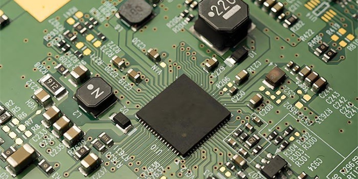
The Printed Circuit Assembly processing workflow encompasses several critical stages: circuit board design, raw material preparation, PCB manufacturing, component placement, soldering, quality inspection, program downloading, packaging and logistics, and after-sales service. These stages form the foundation of the electronics manufacturing industry and significantly impact product quality and innovation. Each stage requires stringent quality control to ensure optimal product performance.
1. Circuit Board Design
The first step in PCBA processing is circuit board design. During this phase, electronic engineers use specialized PCB design software such as Altium Designer and KiCad to create circuit diagrams and schematics. Key considerations during the design phase include the board’s size, shape, layer count, inter-layer connections, and component layout. Each design decision directly affects the complexity of subsequent processing and the final product’s performance.
2. Raw Material Preparation
Following the design phase, raw material preparation involves sourcing components, manufacturing PCB boards, and preparing solder and plating materials. Components are procured based on the BOM (Bill of Materials) to ensure accuracy. PCB manufacturing involves complex processes such as etching, drilling, and plating, each requiring precise control to ensure the board’s conductivity and stability.
3. PCB Manufacturing
PCB manufacturing is one of the core stages of PCBA processing. This stage includes printing, etching, drilling, plating, and coating pads. These processes involve accurately transferring the circuit pattern onto the PCB substrate to create conductive pathways. High precision and adherence to operational standards are critical, as even minor deviations can impact the board's performance.
4. Component Placement
Component placement involves securing electronic components onto the PCB. Two primary techniques are used: Surface Mount Technology (SMT) and Through-Hole Technology (THT). SMT is suited for small components like resistors and capacitors and is performed automatically using pick-and-place machines. THT is used for larger or specialized components such as sockets and connectors and typically requires manual or automated insertion machines.
5. Soldering
Soldering is a crucial step for securing components to the PCB. Common soldering methods include reflow soldering and wave soldering. Reflow soldering involves melting solder paste at high temperatures to form strong connections between components and the PCB. Wave soldering is used primarily for THT components. Quality control of soldering parameters and processes is essential, as soldering quality directly affects the board’s reliability and stability.
6. Quality Inspection
A quality inspection ensures the PCBA processing quality. This involves both visual inspections and functional testing. Visual inspections focus on soldering quality, checking for issues such as short circuits or solder voids. Functional testing uses specialized equipment to verify that the PCB operates according to design specifications. Defective products are either repaired or discarded to ensure final product quality.
7. Program Downloading
Once PCBA processing is complete, control programs must be downloaded onto the relevant chips or modules, enabling the PCB to operate as programmed. This step is crucial for smart electronic products, as it directly affects the product’s functionality and user experience.
8. Packaging and Logistics
Completed PCBs need proper packaging to prevent damage during transportation and storage. Selecting appropriate packaging materials and logistics methods ensures that products reach customers safely and on time.
9. After-Sales Service
After-sales service involves providing technical support and maintenance to ensure proper product usage. High-quality after-sales service enhances customer satisfaction and helps manufacturers build a positive reputation and market credibility.
Conclusion
The PCBA processing workflow is a complex and detailed process involving circuit board design, raw material preparation, PCB manufacturing, component placement, soldering, quality inspection, program downloading, packaging and logistics, and after-sales service. Each stage requires rigorous quality control and engineering support to ensure the final product meets customer expectations.
Through this detailed analysis, you should have a comprehensive understanding of the PCBA processing stages. As the electronics manufacturing industry continues to evolve, PCBA technology will play a crucial role in driving innovation and upgrading electronic products. Gekunflex remains committed to supporting high-quality PCBA solutions, ensuring that your electronic products achieve optimal performance and reliability.


