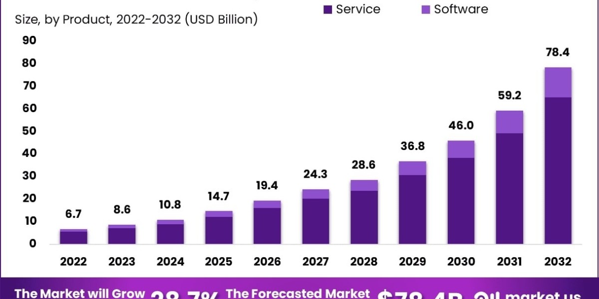
Global CMP Slurry Monitoring Market size was valued at US$ 183.4 million in 2024 and is projected to reach US$ 326.7 million by 2032, at a CAGR of 8.5% during the forecast period 2025-2032. The U.S. market is estimated at USD 92.4 million in 2024, while China is expected to grow at a faster pace reaching USD 134.6 million by 2032.
CMP (Chemical Mechanical Planarization) slurry monitoring systems are critical quality control solutions used in semiconductor manufacturing to analyze and maintain slurry properties. These systems measure key parameters including Large Particle Counts (LPC), density, viscosity, pH levels, and particle size distribution to ensure optimal polishing performance. The technology plays a vital role in improving wafer yield and reducing defects in advanced node semiconductor production.
Market growth is driven by the semiconductor industry’s transition to smaller process nodes (below 7nm) which requires stricter slurry quality control. The Large Particle Counts (LPC) segment dominates with 38% market share in 2024 due to its direct impact on wafer surface defects. Key players like ENTEGRIS, INC and HORIBA are expanding their monitoring portfolios through acquisitions, with the top five companies holding 62% market share. Recent innovations include real-time monitoring systems that integrate AI for predictive maintenance in fab operations.
Get Full Report : https://semiconductorinsight.com/report/cmp-slurry-monitoring-market/
MARKET DYNAMICS
MARKET DRIVERS
Rising Demand for Advanced Semiconductor Manufacturing to Boost CMP Slurry Monitoring Adoption
The global semiconductor industry is experiencing unprecedented growth, with manufacturing complexity increasing as chip designs shrink below 10nm nodes. This drives the need for precise chemical mechanical planarization (CMP) processes where slurry quality directly impacts yield rates. Leading foundries report that improper slurry monitoring can reduce wafer yields by up to 15-20% due to defects like scratching or incomplete polishing. As a result, semiconductor manufacturers are increasingly adopting automated CMP slurry monitoring systems to maintain optimal particle size distribution, viscosity, and chemical composition throughout the polishing process.
Technology Miniaturization Trends Accelerating Market Growth
The relentless push toward smaller semiconductor nodes below 7nm is creating new challenges in CMP processes that require real-time slurry monitoring. Modern slurry formulations contain engineered abrasives with particle sizes under 100nm, where even minor deviations in particle concentration can cause catastrophic wafer defects. This technological evolution has led to a threefold increase in demand for advanced monitoring solutions capable of detecting sub-100nm particles across multiple CMP process steps. Leading manufacturers now integrate monitoring systems directly into CMP tools to enable closed-loop control, driving market growth as foundries upgrade equipment for next-generation nodes.
Increasing Focus on Predictive Maintenance Creating New Opportunities
Semiconductor manufacturers are shifting from reactive to predictive maintenance strategies, with CMP slurry monitoring playing a pivotal role. Continuous monitoring of slurry parameters allows for early detection of quality degradation before it impacts production. Analysis shows that predictive maintenance enabled by slurry monitoring can reduce unplanned tool downtime by 30-40% while extending consumable lifecycles. Major players now offer AI-powered analytics platforms that correlate slurry data with tool performance, helping fabs optimize polish rates and reduce material waste. This trend is particularly strong in memory chip production, where CMP processes account for over 25% of total manufacturing costs.
MARKET RESTRAINTS
High Implementation Costs Creating Barriers for Smaller Fabs
While CMP slurry monitoring delivers substantial ROI for high-volume manufacturers, the capital expenditure required creates significant barriers for adoption. A complete monitoring system including sensors, analytics software, and integration with CMP tools can cost $500,000-$1 million per toolset. This represents a major investment for smaller foundries or research facilities that may process fewer wafers. Additionally, the need for specialized installation and calibration further increases total cost of ownership, limiting market penetration among cost-sensitive operations.
Technical Complexity of Multi-Parameter Monitoring Presents Challenges
Modern CMP slurries require monitoring of 10+ critical parameters simultaneously, including particle counts, zeta potential, pH, and chemical concentrations. Integrating sensors for all relevant measurements without disrupting slurry flow or introducing measurement artifacts remains an engineering challenge. Many existing monitoring solutions compromise by measuring only 2-3 key parameters, potentially missing critical quality variations. The industry also faces difficulties in developing non-invasive sensors that can withstand the corrosive chemical environment of CMP slurries over extended periods without drift or contamination.
Lack of Standardization Across Slurry Formulations
The CMP slurry market includes hundreds of proprietary formulations from different suppliers, each requiring customized monitoring approaches. This lack of standardization forces equipment vendors to develop numerous sensor configurations and calibration methods. Foundries using multiple slurry types face additional complexity in maintaining separate monitoring protocols for each chemistry. The situation is particularly challenging for advanced materials like ceria-based slurries where oxidation state monitoring becomes critical but lacks established industry standards.
MARKET OPPORTUNITIES
Emerging Advanced Packaging Technologies Creating New Application Areas
The rapid growth of advanced packaging technologies like 3D IC and chiplets is opening new applications for CMP slurry monitoring. These packaging approaches require planarization of multiple material layers including copper, dielectrics, and through-silicon vias (TSVs). Each material combination demands specialized slurry formulations with tight process control. Market analysis indicates the packaging segment will grow at a 12-15% CAGR as next-generation devices increasingly adopt heterogeneous integration. This creates opportunities for monitoring solutions that can handle the diverse material sets used in advanced packaging workflows.
AI-Powered Analytics Transforming Slurry Process Control
The integration of machine learning with CMP slurry monitoring represents a major growth opportunity. Advanced algorithms can now predict slurry degradation patterns and optimize replenishment schedules with 90-95% accuracy. This enables significant reductions in slurry consumption while minimizing quality excursions. Leading manufacturers are developing cloud-based platforms that aggregate data across multiple fabs to identify global optimization opportunities. These AI solutions are particularly valuable for memory manufacturers where small improvements in CMP efficiency can translate to millions in annual savings.
Expansion in Compound Semiconductor Manufacturing
The growing production of compound semiconductors for power electronics, RF devices, and photonics is creating new markets for specialized CMP monitoring solutions. Materials like GaN and SiC present unique planarization challenges due to their hardness and chemical stability. The compound semiconductor market is projected to grow at 18-20% annually as electric vehicle and 5G adoption accelerates. This drives demand for monitoring systems capable of handling the aggressive chemistries and high-pressure conditions required for compound semiconductor CMP processes.
MARKET CHALLENGES
Maintaining Measurement Accuracy in High-Volume Production
Ensuring consistent monitoring accuracy across thousands of wafer polishing cycles remains a significant challenge. Sensor drift, slurry residue buildup, and calibration inconsistencies can degrade measurement precision by 10-15% between maintenance cycles. This variability creates quality control risks as manufacturers push CMP tools to higher throughput levels. The industry is responding with self-calibrating sensors and automated cleaning systems, but achieving six-sigma reliability in production environments continues to challenge equipment developers.
Integration Challenges with Legacy CMP Equipment
Many semiconductor fabs operate CMP tools that are 7-10 years old, lacking modern interfaces for real-time monitoring integration. Retrofitting these systems with advanced slurry monitoring capabilities often requires extensive tool modifications that can cost $200,000+ per tool. The compatibility issues create adoption barriers as manufacturers weigh the benefits against potential production disruptions during installation. Equipment vendors are developing modular solutions to ease integration, but the diverse installed base continues to present technical challenges.
Environmental Regulations Impacting Slurry Formulations
Increasing environmental regulations are forcing changes to CMP slurry chemistries, particularly regarding heavy metal content and wastewater discharge. Each formulation change requires corresponding updates to monitoring protocols and sensor configurations. The EU’s recent restrictions on certain abrasive materials have already impacted 15-20% of traditional slurry formulations. These regulatory shifts create uncertainty as monitoring system providers must continuously adapt to evolving material restrictions while maintaining measurement accuracy across changing chemistries.
CMP SLURRY MONITORING MARKET TRENDS
Increasing Semiconductor Manufacturing Complexity Driving Demand for Advanced CMP Slurry Monitoring
The semiconductor industry’s relentless push toward smaller node sizes below 7nm has significantly increased the importance of precise Chemical Mechanical Planarization (CMP) slurry monitoring. As feature sizes shrink below 5nm, particle contamination becomes exponentially more critical, with even nanometer-scale impurities capable of causing device failures. This technological imperative has driven adoption rates of advanced slurry monitoring systems to over 65% among leading semiconductor foundries. The integration of real-time analytics with IoT-connected monitoring devices allows for immediate corrective actions, reducing wafer scrap rates by approximately 25%. Furthermore, the emergence of artificial intelligence and machine learning applications in slurry monitoring has enabled predictive maintenance capabilities, further enhancing yield optimization.
Other Trends
Transition to Copper Interconnects and New Materials
The industry-wide transition from aluminum to copper interconnects and the adoption of novel low-k dielectric materials have introduced new challenges in CMP processing. Copper slurry monitoring now accounts for nearly 40% of total monitoring system deployments, requiring specialized capabilities to detect electrochemical interactions and maintain optimal oxidation states. Additionally, the introduction of cobalt interconnect technology in advanced nodes has created demand for monitoring solutions capable of tracking multiple slurry parameters simultaneously, including pH levels, oxidation-reduction potential, and abrasive particle distribution.
Expansion of 300mm Wafer Fabs and Emerging 450mm Transition
The continued expansion of 300mm wafer manufacturing facilities worldwide has created substantial demand for slurry monitoring systems. With approximately 130 operational 300mm fabs globally and 20 more under construction, monitoring equipment must handle higher throughput requirements while maintaining precision. Meanwhile, pilot lines for 450mm wafer processing are driving development of next-generation monitoring solutions capable of handling larger slurry volumes and more complex fluid dynamics. This transition presents both challenges and opportunities in slurry monitoring, requiring innovations in sensor technology and data processing capabilities to ensure consistent performance across larger wafer surfaces.
Increasing Regulatory Scrutiny on Environmental Compliance
Stringent environmental regulations governing chemical usage and waste management in semiconductor manufacturing are prompting greater investment in comprehensive slurry monitoring solutions. Facilities are implementing closed-loop systems that reduce chemical consumption by up to 30% while maintaining process quality. Advanced monitoring technologies now track not only slurry composition during use but also degradation byproducts for proper disposal classification. This regulatory pressure, combined with corporate sustainability initiatives, has made environmental monitoring capabilities a key differentiator in slurry monitoring system procurement decisions.
COMPETITIVE LANDSCAPE
Key Industry Players
Innovative Monitoring Solutions Reshape the Competitive Dynamics
The global CMP Slurry Monitoring market exhibits a moderately consolidated structure dominated by specialized technology providers catering to semiconductor fabrication needs. ENTEGRIS, INC leads the competitive landscape with approximately 22% market share in 2024, owing to its comprehensive portfolio of real-time slurry monitoring systems and strong partnerships with leading foundries.
HORIBA and Rheonics collectively account for nearly 30% of the market, leveraging their expertise in precision measurement technologies. These companies gained significant traction through their ability to integrate viscosity monitoring with particle counting capabilities – a critical advancement for 3nm and below process nodes.
Recent developments show competitors accelerating R&D investments to address emerging requirements. Spheryx, Inc. made strategic moves in 2023 with its patented xSight system that offers inline zeta potential measurements alongside traditional LPC detection – a functionality gaining importance in advanced node production.
Meanwhile, Colloidal Dynamics LLC strengthened its position through the 2022 acquisition of Nanolytica’s spectroscopy patents, enhancing its multi-parameter analysis capabilities. The company currently holds about 12% of the global monitoring solutions market.
List of Leading CMP Slurry Monitoring Solution Providers
- ENTEGRIS, INC (U.S.)
- Rheonics (Switzerland)
- Colloidal Dynamics LLC (U.S.)
- HORIBA (Japan)
- Entegris (U.S.)
- Spheryx, Inc. (U.S.)
- Applied Analytics, Inc. (U.S.)
Segment Analysis:
By Type
Large Particle Counts (LPC) Segment Dominates Due to Critical Role in Semiconductor Quality Control
The market is segmented based on type into:
- Large Particle Counts (LPC)
- Subtypes: In-line sensors and off-line analyzers
- Density
- Viscosity
- Others
By Application
Semiconductor Manufacturing Segment Leads Owing to Rising Demand for Advanced Chip Fabrication
The market is segmented based on application into:
- Integrated Circuit
- Semiconductor Manufacturing
- Others
By End User
Foundries Dominate Market Share Due to High-Volume Production Requirements
The market is segmented based on end user into:
- Foundries
- IDMs (Integrated Device Manufacturers)
- Research Institutions
Regional Analysis: CMP Slurry Monitoring Market
North America
The North American CMP slurry monitoring market is thriving due to robust semiconductor manufacturing and significant investments in advanced wafer fabrication technologies. The U.S., in particular, holds a dominant position, accounting for over 40% of the regional market share. Key semiconductor hubs such as Silicon Valley and Arizona drive demand for real-time slurry monitoring systems that optimize chemical mechanical planarization (CMP) processes. Strict quality control standards set by semiconductor giants like Intel and Micron intensify the need for high-precision monitoring of slurry properties, including Large Particle Counts (LPC) and viscosity. Rising adoption of Industry 4.0 and IoT-enabled monitoring solutions further accelerates growth in this region. Challenges include high costs of advanced monitoring equipment, though these are offset by strong R&D investments from leading players.
Europe
Europe’s market is driven by a combination of environmental regulations and demand for high-performance semiconductor manufacturing. Countries like Germany and Belgium—home to major fabrication plants—are investing in automated slurry-monitoring solutions to enhance production efficiency. EU directives on waste reduction and chemical sustainability push manufacturers toward slurry-monitoring technologies that minimize defects and optimize slurry usage. High labor costs in Europe make automation particularly appealing, fostering growth opportunities for vendors offering AI-driven monitoring systems. However, smaller semiconductor manufacturers in Eastern Europe face cost-related barriers, slowing adoption in those areas. Collaboration between research institutions and industry players is addressing these hurdles while maintaining compliance with stringent regulatory frameworks.
Asia-Pacific
Asia-Pacific dominates the global CMP slurry monitoring market, accounting for over 50% of global revenues as of 2024. China, Taiwan, and South Korea lead due to massive semiconductor production capacity—Taiwan’s TSMC alone contributes significantly to regional demand. The rapid expansion of new semiconductor fabs, particularly in China, fuels adoption of density and viscosity monitoring tools. However, cost sensitivity among smaller foundries in Southeast Asia still favors manual monitoring, restricting penetration in some markets. Government initiatives like India’s Semiconductor Mission and Japan’s subsidies for domestic chip production are expected to further accelerate demand. Meanwhile, South Korea’s Samsung and SK Hynix drive innovations in slurry reuse, necessitating highly precise monitoring solutions.
South America
The South American market remains nascent, hindered by limited semiconductor manufacturing infrastructure. Brazil shows marginal growth potential due to investments in electronic component production, but overall adoption of CMP slurry monitoring technologies is low. Economic instability and reliance on imported chips discourage capital-intensive slurry monitoring investments. However, multinational companies expanding assembly operations in Mexico and Argentina are gradually introducing basic monitoring tools to improve yield rates. Regulatory frameworks for chemical handling remain underdeveloped, slowing adoption of advanced slurry management systems. Despite these challenges, long-term opportunities exist if local governments prioritize semiconductor industry development.
Middle East & Africa
This region represents an emerging market with focused growth in select countries like Israel and the UAE. While semiconductor manufacturing is limited, Israel’s tech-driven economy fosters demand for slurry monitoring in specialized IC production. The UAE’s push for industrial diversification, including semiconductor packaging, presents niche opportunities. However, the lack of large-scale wafer fabs and reliance on imports constrain market expansion. Recent collaborations between Middle Eastern governments and global semiconductor firms hint at future potential, particularly in smart city projects requiring localized chip production. High costs and technical skill gaps remain barriers though, limiting immediate growth.
Get A Sample Report : https://semiconductorinsight.com/download-sample-report/?product_id=97732
Report Scope
This market research report provides a comprehensive analysis of the global and regional CMP Slurry Monitoring markets, covering the forecast period 2025–2032. It offers detailed insights into market dynamics, technological advancements, competitive landscape, and key trends shaping the industry.
Key focus areas of the report include:
- Market Size & Forecast: Historical data and future projections for revenue, unit shipments, and market value across major regions and segments. The global CMP Slurry Monitoring market was valued at USD million in 2024 and is projected to reach USD million by 2032, at a CAGR of % during the forecast period.
- Segmentation Analysis: Detailed breakdown by product type (Large Particle Counts (LPC), Density, Viscosity, Others), application (Integrated Circuit, Semiconductor Manufacturing, Others), and end-user industry to identify high-growth segments and investment opportunities.
- Regional Outlook: Insights into market performance across North America (U.S., Canada, Mexico), Europe (Germany, France, U.K.), Asia-Pacific (China, Japan, South Korea), Latin America, and the Middle East & Africa, including country-level analysis.
- Competitive Landscape: Profiles of leading market participants including ENTEGRIS, INC, Rheonics, Colloidal Dynamics LLC, HORIBA, Entegris, Spheryx, Inc., and Applied Analytics, Inc., covering their product offerings, market share (top five players held approximately % share in 2024), and recent developments.
- Technology Trends & Innovation: Assessment of emerging monitoring technologies, integration of AI/IoT in slurry monitoring, and evolving semiconductor fabrication standards.
- Market Drivers & Restraints: Evaluation of factors driving market growth along with challenges in semiconductor manufacturing processes, supply chain constraints, and technical barriers.
- Stakeholder Analysis: Insights for component suppliers, semiconductor manufacturers, equipment OEMs, investors, and policymakers regarding the evolving ecosystem and strategic opportunities.
Primary and secondary research methods are employed, including interviews with industry experts, data from verified sources, and real-time market intelligence to ensure the accuracy and reliability of the insights presented.
Customisation of the Report
In case of any queries or customisation requirements, please connect with our sales team, who will ensure that your requirements are met.
Related Reports :
https://semiconductorinsight.com/report/12-inch-semiconductor-silicon-wafer-market/
https://semiconductorinsight.com/report/global-gesture-sensor-market/
https://semiconductorinsight.com/report/iris-recognition-access-control-system-market/
https://semiconductorinsight.com/report/thermistor-temperature-sensor-market-2/
https://dineshsemiconductorsinsightspr.blogspot.com/2025/06/inverted-light-microscopy-market.html
https://dineshsemiconductorsinsightspr.blogspot.com/2025/06/binary-gas-analyser-market-business.html
https://dineshsemiconductorsinsightspr.blogspot.com/2025/06/low-dropout-ldo-linear-voltage.html
https://dineshsemiconductorsinsightspr.blogspot.com/2025/06/vcsel-laser-diode-market-emerging.html
https://dineshsemiconductorsinsightspr.blogspot.com/2025/06/boat-monitoring-and-control-systems.html
https://dineshsemiconductorsinsightspr.blogspot.com/2025/06/automotive-shunt-resistors-market.html
https://dineshsemiconductorsinsightspr.blogspot.com/2025/06/fbg-packaged-sensor-market-global.html
Contact us:
help@semiconductorinsight.com