Electronic grade silicon wafers are ultra-pure silicon substrates used as the foundation for semiconductor devices. These wafers undergo stringent manufacturing processes to achieve impurity levels below 1 part per billion, making them essential for integrated circuits, memory chips, and power devices. The wafers are classified by diameter sizes including 150mm (6-inch), 200mm (8-inch), and 300mm (12-inch), with the latter dominating production due to superior economies of scale.
The market growth is driven by accelerating demand for advanced semiconductors across artificial intelligence, 5G infrastructure, and electric vehicles. While the 300mm wafer segment leads adoption, emerging applications in quantum computing and IoT sensors are creating new opportunities. Recent capacity expansions by key players like GlobalWafers’ USD 5 billion investment in new 300mm fabs and SUMCO’s long-term supply agreements with major foundries underscore the industry’s bullish outlook.
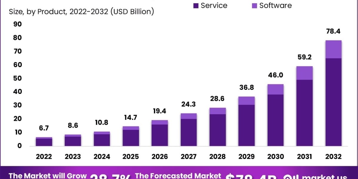
Get Full Report with trend analysis, growth forecasts, and Future strategies : https://semiconductorinsight.com/report/global-electronic-grade-silicon-wafer-market/
Segment Analysis:
By Type
300mm Wafer Segment Dominates Due to High Demand in Advanced Semiconductor Manufacturing
The market is segmented based on type into:
- 150mm
- 200mm
- 300mm
By Application
Logic and MPU Segment Leads with Strong Growth in Processor Manufacturing
The market is segmented based on application into:
- Memory
- Logic and MPU
- Analog
- Discrete Device & Sensor
- Other
By End User
Foundries Remain Primary Consumers Due to Increasing Chip Manufacturing
The market is segmented based on end user into:
- Foundries
- Integrated Device Manufacturers (IDMs)
- Research Institutions
By Fabrication Technology
Epitaxial Wafers Gain Traction for High-Performance Applications
The market is segmented based on fabrication technology into:
- Polished Wafers
- Epitaxial Wafers
- SOI Wafers
Regional Analysis: Global Electronic Grade Silicon Wafer Market
North America
The North American electronic grade silicon wafer market is characterized by strong demand from the semiconductor and electronics industries, particularly in the U.S. and Canada. Investments in advanced semiconductor manufacturing, such as the CHIPS and Science Act allocating $52 billion for domestic semiconductor production, are driving growth. The region is a hub for cutting-edge technology development, increasing demand for 300mm wafers used in high-performance computing and AI applications. However, challenges include supply chain constraints and competition from Asia-based manufacturers. Key players like WaferWorks and SUMCO have a significant presence through partnerships with U.S. semiconductor firms.
Europe
Europe’s market is supported by strong government initiatives like the European Chips Act, which aims to double the EU’s semiconductor production share to 20% by 2030. Countries like Germany, France, and the Netherlands are leading the way in semiconductor R&D, fostering demand for high-purity silicon wafers. The region emphasizes sustainable semiconductor manufacturing, pushing innovations in wafer recycling and energy-efficient production. However, reliance on imports for raw materials and competition from Asia-Pacific manufacturers remain challenges. Siltronic, headquartered in Germany, plays a pivotal role in the European supply chain.
Asia-Pacific
The largest and fastest-growing electronic grade silicon wafer market, Asia-Pacific is dominated by China, Japan, South Korea, and Taiwan. China’s aggressive semiconductor self-sufficiency push, including a $150 billion investment in domestic semiconductor capabilities, is shaping demand. Japan and South Korea remain leaders in wafer manufacturing, with companies like SUMCO and Siltronic supplying global chipmakers. The region’s strong foundry ecosystem, led by TSMC and Samsung, ensures steady demand for 300mm wafers. However, geopolitical factors and export restrictions on advanced wafer technology pose risks to long-term market expansion.
South America
The South American market is nascent but growing, with Brazil leading in semiconductor packaging and testing operations. While wafer production remains limited, increasing foreign investments in Brazil and Argentina signal gradual market development. Challenges include infrastructure limitations and reliance on imported wafers from Asia and North America. Recent government initiatives to boost local electronics manufacturing could drive future demand, though adoption of advanced wafer technologies lags behind global trends.
Middle East & Africa
This emerging market is witnessing strategic investments in semiconductor infrastructure, particularly in the UAE and Saudi Arabia as part of broader technology diversification plans. While wafer production capacity is minimal, growing demand from consumer electronics and telecom sectors presents opportunities. South Africa shows potential with its established electronics industry, though economic constraints limit rapid expansion. The region’s focus on developing downstream semiconductor applications may gradually increase wafer demand, particularly for 200mm and smaller diameter products used in power electronics.
MARKET OPPORTUNITIES
Advanced Packaging Technologies to Create New Wafer Demand Segments
The semiconductor industry’s shift toward advanced packaging solutions presents significant growth potential for specialized wafer products. Heterogeneous integration approaches like chiplets and 3D stacking require ultra-thin wafers with enhanced mechanical properties, commanding premium pricing. The market for thin wafers used in fan-out wafer-level packaging is expanding rapidly, with annual growth projections exceeding 18% as packaging becomes a key differentiator in semiconductor performance.
Emerging Applications in Power Electronics to Drive Market Diversification
Electric vehicles and renewable energy systems are creating substantial demand for specialized wafers optimized for power devices. Silicon carbide wafers for high-voltage applications represent particularly strong growth potential, though production scaling remains challenging. Manufacturers developing innovative crystal growth techniques for compound semiconductor materials are well-positioned to capitalize on this shift toward energy-efficient power electronics.
ELECTRONIC GRADE SILICON WAFER MARKET TRENDS
Rising Demand for 300mm Wafers to Drive Market Expansion
The global electronic grade silicon wafer market is experiencing significant growth, primarily driven by the increasing demand for 300mm wafers across semiconductor fabrication facilities. As the technology nodes shrink below 7nm, larger wafer sizes have become essential for maintaining cost efficiency in chip manufacturing. Currently, nearly 70% of all semiconductor devices are produced on 300mm wafers, with this segment projected to maintain its dominance through 2028. The transition to larger diameters has been accelerated by the need for higher die yields and reduced production costs per chip, particularly in advanced logic and memory applications.
Other Trends
Proliferation of IoT and 5G Technologies
The rapid deployment of 5G networks and the exponential growth of IoT devices are creating unprecedented demand for high-purity silicon wafers. Each 5G base station requires significantly more semiconductor content than previous generations, while IoT sensors are being deployed at a rate exceeding 40 billion units annually. This surge is directly translating to increased wafer consumption across foundries and IDMs. Furthermore, the transition to millimeter-wave frequencies in 5G NR is driving adoption of specialized silicon-on-insulator (SOI) wafers for RF applications.
Geographic Shift in Semiconductor Manufacturing
The market is witnessing a notable geographic realignment of wafer demand as semiconductor manufacturing expands beyond traditional hubs. While Asia-Pacific continues to dominate with over 80% of global wafer production capacity, substantial investments in North America and Europe are reshaping the supply landscape. Recent CHIPS Act funding in the United States and similar initiatives in the EU are accelerating domestic wafer capacity expansions, with at least 12 major new fabs planned through 2026. This geographic diversification is creating new opportunities for wafer suppliers while introducing complexities in global supply chain logistics.
Advanced Packaging Technologies Reshaping Demand
Emerging 3D packaging technologies such as chiplet architectures and fan-out wafer-level packaging are creating new demand patterns for electronic grade silicon wafers. These advanced packaging approaches often require specialized wafer types with ultra-flat surfaces and specific crystalline orientations. The market for interposer wafers used in 2.5D packaging is projected to grow at a CAGR of 18% through 2027, outpacing the overall wafer market. Additionally, the rise of heterogeneous integration is driving innovation in wafer-level testing and metrology solutions.
COMPETITIVE LANDSCAPE
Key Industry Players
Leading Manufacturers Focus on Technological Advancements to Maintain Market Dominance
The global electronic grade silicon wafer market exhibits an oligopolistic structure, dominated by a handful of major players controlling approximately 80% of the market share as of 2023. SUMCO Corporation and Shin-Etsu Chemical (SEH) collectively account for nearly 50% of the worldwide production capacity, benefiting from their vertical integration strategies and long-standing relationships with semiconductor manufacturers.
Siltronic AG and GlobalWafers have emerged as strong competitors in recent years, particularly in the 300mm wafer segment which represents over 70% of industry revenue. Their growth can be attributed to strategic capacity expansions in Asia-Pacific regions and partnerships with foundries developing advanced process nodes.
The competitive intensity has increased significantly with Chinese players like Zhonghuan Semiconductor and National Silicon Industry Group (NSIG) aggressively expanding their market presence through government-backed initiatives. While currently holding smaller market shares, these companies are expected to account for 25-30% of global capacity by 2027 according to industry projections.
Market leaders continue to invest heavily in R&D for larger wafer sizes (450mm development) and specialty substrates like silicon-on-insulator (SOI) to maintain technological leadership. The recent acquisition of Siltronic by GlobalWafers for €3.8 billion underscores the strategic importance of consolidation in this capital-intensive industry.
List of Key Electronic Grade Silicon Wafer Manufacturers
- Shin-Etsu Chemical Co., Ltd. (SEH) (Japan)
- SUMCO Corporation (Japan)
- Siltronic AG (Germany)
- GlobalWafers Co., Ltd. (Taiwan)
- SK Siltron (South Korea)
- Wafer Works Corporation (Taiwan)
- Ferrotec Holdings Corporation (Japan)
- AST (Advanced Semiconductor Materials) (U.S.)
- NSIG (National Silicon Industry Group) (China)
Learn more about Competitive Analysis, and Forecast of Global Electronic Grade Silicon Wafer Market : https://semiconductorinsight.com/download-sample-report/?product_id=95804
FREQUENTLY ASKED QUESTIONS:
What is the current market size of Global Electronic Grade Silicon Wafer Market?
-> Electronic Grade Silicon Wafer Market size was valued at US$ 16.73 billion in 2024 and is projected to reach US$ 28.46 billion by 2032, at a CAGR of 6.4% during the forecast period 2025-2032.
Which key companies dominate the silicon wafer market?
-> Top five players (Shin-Etsu, SUMCO, GlobalWafers, Siltronic, SK Siltron) control approximately 85% of global production capacity.
What are the primary growth drivers?
-> Key drivers include semiconductor industry expansion, increasing 300mm wafer adoption, and growing demand for advanced logic and memory chips.
Which region leads in silicon wafer production?
-> Asia-Pacific accounts for 78% of global wafer production, with Japan, South Korea, and Taiwan as major hubs.
What are the key technology trends?
-> Emerging trends include larger 450mm wafer development, epitaxial wafer adoption, and advanced defect control technologies for sub-7nm nodes.
CONTACT US:
City vista, 203A, Fountain Road, Ashoka Nagar, Kharadi, Pune, Maharashtra 411014
+91 8087992013
help@semiconductorinsight.com
Follow us on LinkedIn: https://www.linkedin.com/company/semiconductor-insight/