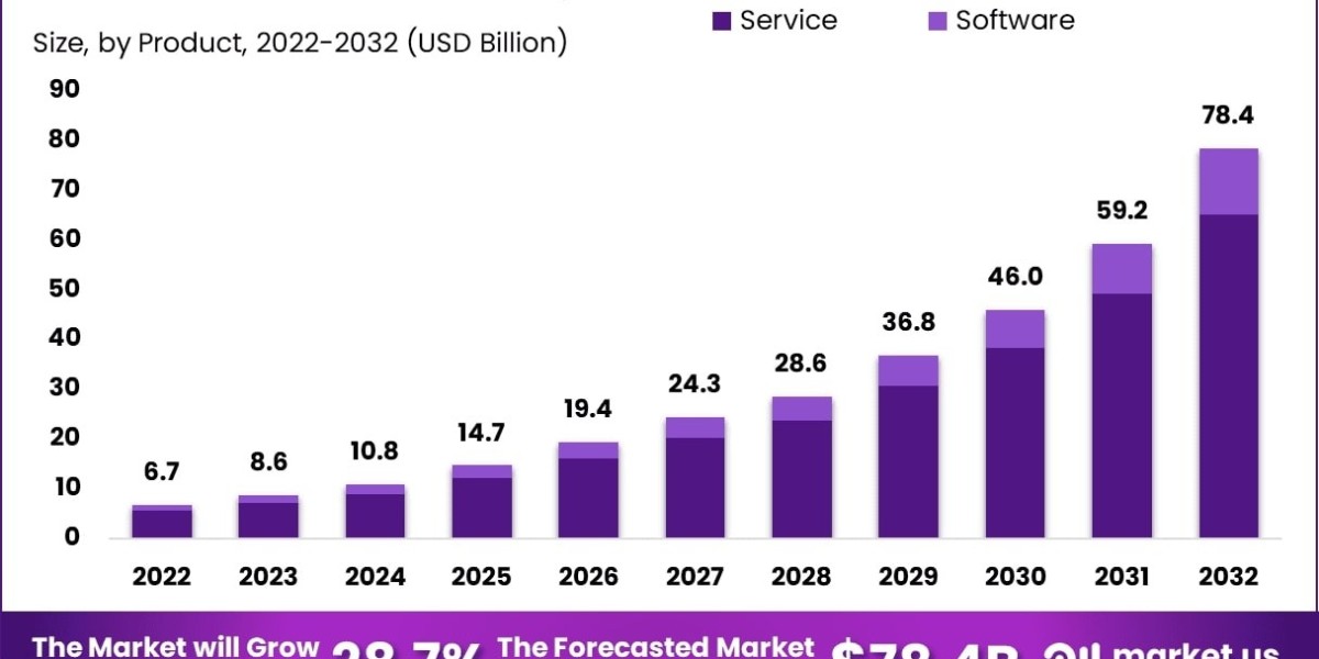
The global semiconductor metrology and inspection equipment market was valued at USD 8.98 billion in 2024 and is expected to reach USD 16.21 billion by 2033, growing at a CAGR of 6.9% from 2025 to 2033. This steady growth is driven by the increasing complexity of semiconductor device architectures—such as FinFETs, Gate-All-Around (GAA), and 3D NAND—which demand advanced inspection and metrology tools to maintain high yield and performance.
Additional factors fueling this growth include the adoption of EUV lithography, rising investments in sub-7nm process technologies, and the ongoing expansion of global fabrication capacity, particularly across Asia-Pacific and North America. These trends are accelerating the demand for high-precision, in-line, and 3D metrology systems.
A significant driver of market momentum is the U.S. government's strong funding initiatives under the CHIPS & Science Act. Since 2022, more than USD 100 million has been allocated toward advanced metrology R&D, with an additional USD 300 million directed toward next-generation packaging metrology in collaboration with NIST and Manufacturing USA. These efforts are enhancing the development of tools capable of managing sub-5nm geometries and reinforcing domestic manufacturing capabilities. The infusion of capital is playing a pivotal role in strengthening foundational research and speeding up commercialization of innovative metrology solutions.
Key Market Insights:
- Regional Insight: Asia Pacific led the global market with a 54.7% revenue share in 2024, attributed to rapid fab expansion and increased investments in high-end process nodes across Taiwan, South Korea, China, and Japan.
- By Technology: The inspection equipment segment held the largest revenue share of 56.8% in 2024, owing to the critical need for early defect detection in advanced semiconductor nodes.
- By Dimension: The 2D metrology/inspection segment accounted for the largest revenue share in 2024. While 2D tools remain dominant in legacy and mid-range nodes, their growth is gradually stabilizing.
- By Process Node: The ≤7 nm segment captured the largest market share in 2024, fueled by the demand for ultra-precise tools required in applications such as high-performance computing (HPC), artificial intelligence (AI), and mobile SoCs.
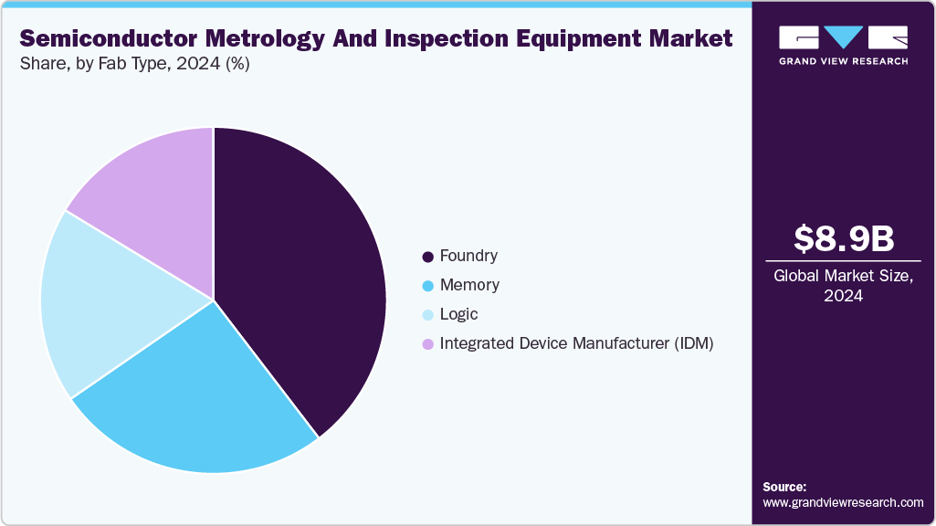
- By Fab Type: Foundries led the market in 2024, supported by diverse customer demand and ongoing transitions to advanced process technologies.
Order a free sample PDF of the Semiconductor Metrology and Inspection Equipment Market Intelligence Study, published by Grand View Research.
Market Size & Forecast
- 2024 Market Size: USD 8.98 Billion
- 2033 Projected Market Size: USD 16.21 Billion
- CAGR (2025-2033): 6.9%
- Asia Pacific: Largest market in 2024
Key Companies & Market Share Insights
Major players in the semiconductor metrology and inspection equipment market include KLA Corporation, Applied Materials, Inc., Hitachi High-Tech Corporation, and ASML. These companies are driving innovation to support sub-7 nm nodes and 3D packaging, developing tools with atomic-scale resolution, real-time defect classification, and integrated metrology for advanced fabs. Many are aligning with national semiconductor initiatives and global standards to ensure scalability and future-readiness.
KLA Corporation is a leader in advanced process control, offering tools like optical and e-beam inspection, CD-SEM, and overlay metrology. It leverages AI-driven analytics to enhance defect detection at sub-5 nm and 3D levels, with strong partnerships in EUV mask and advanced packaging inspection.
Applied Materials, Inc. delivers integrated metrology systems tailored to work with deposition and etch tools. Focused on gate-all-around and 3D packaging, Applied combines quantum sensors and AI to offer real-time feedback and yield enhancement, while actively contributing to advanced inspection standards through R&D collaborations.
Key Players
- Applied Materials, Inc.
- ASML
- Camtek
- Hitachi High-Tech Corporation
- KLA Corporation
- Lasertec Corporation
- Nova Ltd.
- Onto Innovation
- SCREEN Semiconductor Solutions Co., Ltd.
- Thermo Fisher Scientific Inc.
Explore Horizon Databook – The world's most expansive market intelligence platform developed by Grand View Research.
Conclusion
Global semiconductor metrology and inspection equipment market is undergoing substantial growth, propelled by the increasing intricacy of semiconductor architectures. Key drivers include the adoption of advanced lithography techniques, significant investments in new process technologies, and the expansion of fabrication facilities globally. Government initiatives in various countries are also contributing to this expansion by supporting research and development. The Asia Pacific region is a leading player, and technological advancements, such as the integration of AI, are reshaping the industry.