Introduction
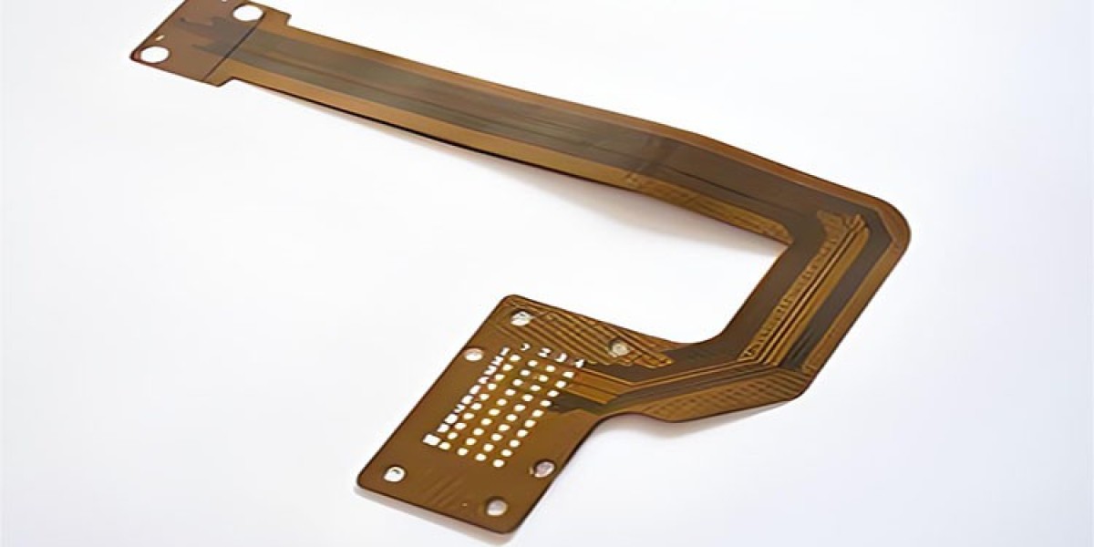
Printed Circuit Boards (PCBs), also known as printed circuits or printed circuit boards, are essential components in modern electronics. A multilayer flexible pcb refers to a circuit board with more than two layers, comprising conductive traces and pads on insulating substrates used for connecting and soldering electronic components. These boards not only provide electrical connections between layers but also offer insulation between them. With the continuous development of Surface Mount Technology (SMT) and the introduction of new Surface Mount Devices (SMDs) like QFP, QFN, CSP, and BGA (especially MBGA), electronic products have become increasingly intelligent and compact. This advancement has driven significant reforms and progress in the PCB industry.
Determining the Board Shape, Dimensions, and Layer Count
Every PCB must fit with other structural components, so the shape and dimensions of the board must align with the overall product structure. However, from a production perspective, the design should be as simple as possible, typically a rectangle with a balanced length-to-width ratio to facilitate assembly, improve production efficiency, and reduce labor costs.
The number of layers is determined by the circuit performance requirements, board size, and trace density. For multilayer PCBs, four-layer and six-layer boards are the most commonly used. A typical four-layer board includes two signal layers (component side and solder side), a power layer, and a ground layer.
The layers of a multilayer board should be symmetrical, and it's preferable to have an even number of copper layers, such as four, six, or eight. Asymmetrical layering can cause the board to warp, which is especially problematic for surface-mount multilayer boards.
Component Placement and Orientation
Component placement and orientation should first be considered from the circuit principle's perspective, following the circuit flow. The rationality of the placement directly affects the PCB's performance, particularly in high-frequency analog circuits, where the placement of components is more stringent. Proper placement of components can, in some sense, predetermine the success of the PCB design. Therefore, when laying out the PCB, it is essential to conduct a detailed analysis of the circuit principle, determine the placement of special components (such as large-scale ICs, high-power transistors, and signal sources), and then arrange other components to minimize potential interference factors.
On the other hand, the overall structure of the PCB should be considered to avoid uneven component distribution or chaotic arrangements, which can affect the board's appearance and complicate assembly and maintenance.
Requirements for Trace Layering and Routing Areas
Generally, multilayer flexible PCB routing is done according to circuit functions. When routing the outer layers, more traces should be on the solder side and fewer on the component side, facilitating PCB maintenance and troubleshooting. Fine, dense traces and easily interfered signal lines are usually placed on the inner layers. Large areas of copper should be evenly distributed on both the inner and outer layers to reduce board warping and ensure uniform plating during the electroplating process. To prevent damage to conductive traces during edge processing and avoid interlayer short circuits during mechanical processing, the distance between the conductive patterns of the inner and outer layers and the board edge should be greater than 50 mils.
Trace Direction and Width Requirements
In multilayer flexible PCBs, the power, ground, and signal layers should be separated to reduce interference between power, ground, and signal traces. Adjacent layers' traces should be perpendicular or routed in diagonal or curved lines to minimize coupling and interference between layers. Traces should be kept as short as possible, especially in small signal circuits, where shorter traces reduce resistance and interference. When signal traces on the same layer change direction, sharp angles should be avoided. Trace width should be determined by the circuit's current and impedance requirements, with power input traces being wider and signal traces narrower. For typical digital boards, the power input trace width should be 50-80 mils, while the signal trace width can be 6-10 mils. It's also important to keep trace width consistent to avoid sudden changes, which helps with impedance matching.
Requirements for Drilled Hole Size and Pads
The size of the component holes on a multilayer PCB depends on the size of the component leads. Holes that are too small will hinder component insertion and soldering, while holes that are too large may result in insufficient solder. Generally, the diameter of component holes and the size of pads are calculated as follows:
- Component hole diameter = Lead diameter (or diagonal) + (10-30 miles)
- Pad diameter ≥ Hole diameter + 18 miles
For vias, the hole diameter is mainly determined by the board's thickness, and for high-density multilayer boards, it should generally be controlled within a thickness-to-hole diameter ratio of ≤ 5:1. The via pad is calculated as follows:
- Via pad diameter ≥ Via diameter + 12 miles
Power and Ground Layer Partitioning and Thermal Relief Requirements
For multilayer PCBs, at least one power layer and one ground layer are required. Since all voltages on the PCB are connected to the same power layer, the power layer must be partitioned for isolation. The partition line width is generally 20-80 mils, with higher voltages requiring thicker lines.
The connection between solder pads and the power and ground layers should be designed with thermal relief pads to increase reliability and reduce the risk of cold solder joints caused by large metal areas absorbing heat during soldering.
- Isolation pad hole diameter ≥ Drill hole diameter + 20 miles
Safety Clearance Requirements
Safety clearance settings should meet electrical safety requirements. Typically, the minimum spacing between outer layer traces should not be less than 4 mils, and the minimum spacing between inner layer traces should not be less than 4 mils. If space permits, the spacing should be as large as possible to improve the yield during board manufacturing and reduce the risk of defects.
Requirements for Enhancing Board-Level Interference Immunity
When designing multilayer PCBs, it is also essential to consider the board's interference immunity. Common methods include:
a. Adding filter capacitors near the power and ground pins of each IC, typically with a capacitance of 473 or 104.
b. Adding guard traces for sensitive signals on the PCB and minimizing traces near the signal source.
c. Choosing reasonable grounding points.
Conclusion
In summary, multilayer PCB design involves a wide range of considerations, and during the design process, attention must be paid to manufacturability and process requirements. Only through continuous practice and experience accumulation can high-quality products be designed. Gekunflex offers professional and high-quality services to meet your multilayer board order requirements with excellent quality.


