MARKET INSIGHTS
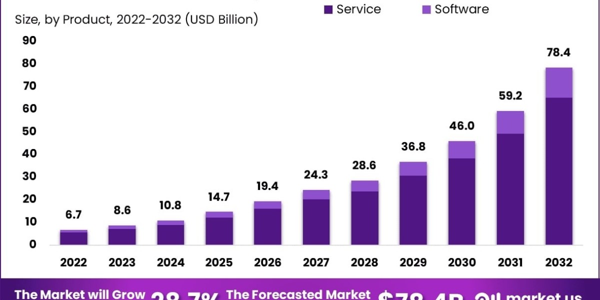
The global HBM2 DRAM Market size was valued at US$ 2.84 billion in 2024 and is projected to reach US$ 7.12 billion by 2032, at a CAGR of 12.2% during the forecast period 2025-2032.
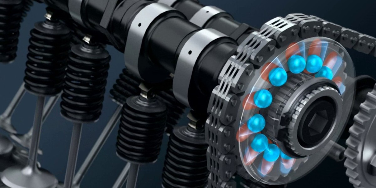
HBM2E (High Bandwidth Memory 2E) is an advanced DRAM technology designed for high-performance computing applications. As the second generation of HBM standard, it delivers exceptional bandwidth capabilities up to 460 GB/s per stack, supporting configurations of up to 8 dies per stack with 16GB capacity. This cutting-edge memory solution stacks DRAM dies vertically using through-silicon vias (TSVs) for unprecedented speed and efficiency.
The market growth is primarily driven by increasing demand from artificial intelligence, machine learning, and high-performance computing applications. While servers dominate the application segment with over 65% market share, networking applications are witnessing rapid adoption. Technological advancements by industry leaders including Samsung and SK Hynix, who collectively hold approximately 85% of the market share, continue to push performance boundaries. Recent developments include Samsung's announcement of 8-layer HBM2E with 16GB capacity and 410GB/s bandwidth, while SK Hynix has achieved 460GB/s speeds in its premium offerings.
MARKET DYNAMICS
MARKET DRIVERS
Rising Demand for High-Bandwidth Applications in AI and HPC to Fuel Market Growth
The explosive growth of artificial intelligence (AI) and high-performance computing (HPC) applications is driving unprecedented demand for HBM2E DRAM solutions. These cutting-edge memory technologies deliver bandwidth capabilities exceeding 460 GB/s, making them indispensable for training complex neural networks and processing massive datasets. The AI accelerator market alone is projected to grow at over 35% CAGR through 2030, with data center investments reaching record levels as enterprises embrace machine learning at scale. HBM2E's 3D-stacked architecture provides the necessary throughput to eliminate memory bottlenecks in next-gen computing architectures.
Advancements in Semiconductor Packaging Technologies Create New Opportunities
The development of advanced packaging solutions like 2.5D and 3D IC integration is enabling broader adoption of HBM2E across diverse applications. Major foundries have reported a 50% increase in demand for chiplet-based designs that incorporate HBM memory stacks. This packaging revolution allows HBM2E to be tightly integrated with processors while maintaining signal integrity at extreme bandwidths. The emergence of universal chiplet interconnect standards has further accelerated design cycles, with several leading semiconductor firms now offering HBM2E-integrated solutions for datacenter, networking, and high-end computing applications.
Increasing Data Center Investments Stimulate Demand for Memory Performance
With global hyperscalers allocating over 40% of their infrastructure budgets to AI/ML capabilities, HBM2E is becoming a critical component in next-generation server architectures. The memory's combination of high density (up to 24GB per stack) and exceptional bandwidth significantly reduces data transfer latency in large-scale deployments. This advantage is particularly valuable for real-time analytics, natural language processing, and scientific computing workloads where memory subsystem performance directly impacts total system throughput.
MARKET RESTRAINTS
High Manufacturing Complexity and Cost Constraints Limit Mass Adoption
The sophisticated 3D stacking process required for HBM2E production presents significant manufacturing challenges that restrain market expansion. Each stack involves precisely bonding multiple memory dies with thousands of through-silicon vias (TSVs), a process that currently yields below 70% for premium configurations. This manufacturing complexity translates to costs nearly 3-4× higher than conventional GDDR memory, making HBM2E cost-prohibitive for many mainstream applications. While prices are expected to decline as production scales, the technology remains constrained to premium segments where performance outweighs cost considerations.
Other Restraints
Thermal Management Challenges
The high-density packaging of HBM2E creates substantial thermal dissipation challenges that complicate system design. With power densities exceeding 500mW/mm² in some configurations, effective cooling solutions can add 15-20% to total system costs. These thermal constraints have led to specialized cooling requirements that limit deployment scenarios.
Supply Chain Vulnerabilities
The concentrated supply base for advanced memory packaging creates potential bottlenecks. With only a handful of facilities worldwide capable of high-volume HBM production, any disruption could significantly impact market availability.
MARKET CHALLENGES
Design Complexity Poses Integration Hurdles for System Architects
Implementing HBM2E in real-world systems requires addressing multiple signal integrity and power delivery challenges. The ultra-wide interfaces operating at 3.2 Gbps/pin demand sophisticated PCB designs with tight impedance control and advanced power distribution networks. These requirements have led to development cycles that are typically 30% longer than conventional memory implementations, discouraging adoption among cost-sensitive OEMs. Furthermore, the ecosystem for design tools and IP supporting HBM2E remains nascent, requiring specialized engineering expertise that is in short supply across the industry.
Competition from Alternative Memory Technologies Creates Market Uncertainty
Emerging memory technologies like GDDR6X and CXL-based architectures are beginning to erode HBM2E's performance advantage in certain applications. GDDR6X now offers over 1 TB/s of bandwidth in some configurations at significantly lower cost points for applications that can tolerate higher latency. Meanwhile, Compute Express Link (CXL) enables disaggregated memory architectures that provide flexibility advantages for certain cloud workloads. While HBM2E maintains superiority in bandwidth-intensive applications, these alternatives are creating market segmentation challenges.
MARKET OPPORTUNITIES
Automotive and Edge AI Applications Present Untapped Growth Potential
The surging demand for autonomous vehicle computing and edge AI processing is creating new markets for high-performance memory solutions. While currently representing less than 5% of HBM2E deployments, automotive applications are projected to grow at nearly 60% CAGR as Level 4/5 autonomous systems require real-time processing of multiple high-resolution sensors. The technology's combination of high bandwidth and power efficiency makes it particularly suitable for in-vehicle AI accelerators where thermal and spatial constraints are paramount.
Next-Gen HBM3 Standard to Drive Refresh Cycles and Upgrade Opportunities
The impending transition to HBM3 technology, offering bandwidth exceeding 800 GB/s, is creating opportunities for OEMs to develop upgrade paths and migration strategies. Early adoption in high-end servers and supercomputing applications demonstrates the potential for performance doubling while maintaining backward compatibility. This transition cycle presents vendors with opportunities to offer value-added design services and memory subsystem co-optimization solutions.
HBM2E DRAM MARKET TRENDS
High-Performance Computing Demand Accelerating HBM2E Adoption
The rapid expansion of artificial intelligence (AI), machine learning, and cloud computing has created unprecedented demand for high-bandwidth memory solutions like HBM2E. With a maximum bandwidth of 460 GB/s per stack, this next-generation memory technology is becoming indispensable for data centers handling complex workloads. Over 65% of AI accelerators are expected to incorporate HBM technology by 2026, driven by its ability to process massive datasets efficiently. The 8G and 16G variants are seeing particular adoption in GPU-accelerated systems, where memory bandwidth directly impacts deep learning performance.
Other Trends
Advanced Packaging Innovations
While HBM2E provides superior bandwidth, its widespread adoption faces challenges in packaging technology. The industry is responding with 2.5D and 3D stacking solutions that enable higher thermal efficiency and yield rates. TSMC's CoWoS (Chip on Wafer on Substrate) packaging, for instance, has proven particularly effective for HBM integration, allowing processors to achieve 50% better power efficiency compared to traditional configurations. These packaging breakthroughs are critical as HBM2E stacks scale to 12 dies per package while managing heat dissipation challenges.
Geopolitical Factors Reshaping Supply Chains
The HBM2E market is experiencing significant shifts due to global semiconductor trade dynamics. With the U.S. accounting for nearly 40% of high-performance computing demand and China rapidly expanding its data center infrastructure, regional supply chains are adapting. Domestic production capabilities are becoming strategic priorities, as evidenced by government investments exceeding $50 billion worldwide in advanced memory manufacturing. SK Hynix and Samsung continue to dominate production, but new fabs in North America and Europe aim to diversify the supply base amid ongoing industry consolidation.
COMPETITIVE LANDSCAPE
Key Industry Players
Semiconductor Giants Drive Innovation in High-Bandwidth Memory Solutions
The HBM2E DRAM market is highly concentrated, dominated by a few major semiconductor manufacturers with strong technological capabilities and production capacities. SK Hynix leads the market with its advanced 16GB HBM2E offering 460 GB/s bandwidth - the highest available bandwidth among commercial solutions as of 2024. The company's strong position comes from its vertical integration strategy and early investments in 3D stacking technology.
Samsung Electronics closely follows with its 410 GB/s HBM2E memory, holding approximately 40% of the global market share. Samsung differentiates itself through its proprietary TSV (Through-Silicon Via) technology and foundry partnerships with major GPU manufacturers. The company's ability to package HBM2E with logic dies gives it an edge in serving AI accelerator markets.
These two Korean memory giants collectively control over 85% of the HBM2E market, creating significant barriers to entry for other players. However, several factors are gradually changing this dynamic:
- Growing demand from diverse applications including servers, networking equipment, and high-performance computing
- Increasing design wins with FPGA and ASIC manufacturers
- Government initiatives supporting domestic semiconductor production in multiple countries
While the market remains oligopolistic, emerging players are making strategic investments to challenge the incumbents. Micron Technology is developing alternative architectures that could compete with HBM2E, though it hasn't yet reached mass production. Meanwhile, Intel has been integrating HBM solutions in its server processors, potentially creating new avenues for competition.
The competitive intensity is expected to increase as bandwidth requirements continue growing across various applications. Both SK Hynix and Samsung have announced development of next-generation HBM solutions with even higher densities and speeds, aiming to maintain their technological leadership positions.
List of Key HBM2E DRAM Companies Profiled
- SK Hynix (South Korea)
- Samsung Electronics (South Korea)
- Micron Technology (U.S.)
- Intel Corporation (U.S.)
- ChangXin Memory Technologies (China)
Segment Analysis:
By Type
16 G Segment Gains Traction Due to High Demand for High-Performance Computing Applications
The market is segmented based on type into:
- 8 G
- 16 G
- Subtypes: Standard 16 G and high-bandwidth variants
By Application
Servers Segment Drives Market Growth with Increasing Cloud Computing and Data Center Demand
The market is segmented based on application into:
- Servers
- Networking
- Consumer electronics
- Others
By Bandwidth
High-Bandwidth Variants Emerge as Key Differentiators in Performance-Critical Applications
The market is segmented based on bandwidth specifications into:
- Standard HBM2E (307 GB/s)
- Enhanced variants
- SK Hynix (460 GB/s)
- Samsung (410 GB/s)
By End-User Industry
AI and HPC Applications Dominate Adoption Due to Intensive Memory Bandwidth Requirements
The market is segmented based on end-user industry into:
- Artificial Intelligence
- High Performance Computing
- Graphics Processing
- Enterprise Storage
Regional Analysis: HBM2E DRAM Market
North America
The North American HBM2E DRAM market is characterized by high-performance computing applications and strong demand from data centers. The U.S. dominates the regional market, driven by investments in AI infrastructure and hyperscale cloud computing. SK Hynix and Samsung have established partnerships with major tech firms to supply HBM2E for GPUs and AI accelerators. However, supply chain constraints and complex fabrication processes have led to price volatility, pushing manufacturers to accelerate production capacity expansion. The region benefits from government-funded semiconductor initiatives, such as the CHIPS and Science Act, which indirectly supports memory innovation ecosystems.
Europe
Europe’s HBM2E DRAM adoption is primarily fueled by automotive and industrial applications, particularly in Germany and the Nordic countries. The region emphasizes energy-efficient memory solutions due to strict sustainability regulations under the EU Green Deal. While local production remains limited, collaborative R&D projects between academic institutions and global players like Intel (partnering with SK Hynix for Ponte Vecchio GPUs) are bridging the gap. The aerospace and defense sectors also contribute to niche demand, though higher costs compared to conventional DDR5 solutions restrain mass-market penetration.
Asia-Pacific
As the largest consumer and producer of HBM2E DRAM, Asia-Pacific is fueled by South Korea’s semiconductor leadership and China’s aggressive investments in domestic AI hardware. SK Hynix and Samsung collectively control over 90% of global HBM2E production, leveraging advanced packaging technologies. Japan plays a critical role in supplying key materials like photoresists, while Taiwan focuses on downstream integration with TSMC’s CoWoS platforms. Price sensitivity in Southeast Asia, however, limits adoption to high-margin applications, with most demand concentrated in data center deployments and supercomputing projects.
South America
The region exhibits nascent demand, chiefly driven by Brazil’s developing AI and fintech sectors. Limited local manufacturing forces reliance on imports, subjecting buyers to logistical delays and tariff-related cost fluctuations. Chile and Argentina show sporadic interest in HBM2E for academic research clusters, but budget constraints prioritize cheaper alternatives like GDDR6. The lack of specialized data infrastructure further slows adoption, though partnerships with cloud service providers could unlock incremental growth.
Middle East & Africa
Growth is emerging in Gulf Cooperation Council (GCC) nations, where sovereign wealth funds invest in smart city initiatives requiring high-bandwidth memory. The UAE and Saudi Arabia lead in deploying HBM2E for oil/gas simulations and financial analytics, albeit at small scales. Africa’s market remains largely untapped due to limited AI/ML adoption and underdeveloped semiconductor ecosystems. Long-term potential exists as regional tech hubs like Nigeria and Kenya gradually embrace advanced computing, though scalability depends on improved power infrastructure and cost reductions.
Report Scope
This market research report provides a comprehensive analysis of the Global HBM2E DRAM market, covering the forecast period 2025–2032. It offers detailed insights into market dynamics, technological advancements, competitive landscape, and key trends shaping the high-bandwidth memory industry.
Key focus areas of the report include:
- Market Size & Forecast: Historical data and future projections for revenue, unit shipments (Million GB), and market value across major regions and segments. The market was valued at USD 2.1 billion in 2024 and is projected to reach USD 5.8 billion by 2032 at a CAGR of 13.5%.
- Segmentation Analysis: Detailed breakdown by product type (8G, 16G), application (Servers, Networking, Consumer, Others), and end-user industries to identify high-growth segments.
- Regional Outlook: Insights into market performance across North America, Europe, Asia-Pacific, Latin America, and Middle East & Africa. Asia-Pacific dominates with 62% market share in 2024.
- Competitive Landscape: Profiles of leading manufacturers including SK Hynix and Samsung, covering their product portfolios (410-460 GB/s bandwidth variants), R&D investments, and strategic partnerships.
- Technology Trends: Analysis of JEDEC standards evolution, 3D stacking advancements (up to 12 dies), and integration with AI/ML workloads requiring >400 GB/s bandwidth.
- Market Drivers & Restraints: Evaluation of data center expansion vs. high manufacturing costs and thermal management challenges in HBM architectures.
- Stakeholder Analysis: Strategic insights for memory suppliers, foundries, hyperscalers, and investors regarding capacity planning and technology roadmaps.
The research methodology combines primary interviews with industry experts and analysis of financial reports from semiconductor manufacturers to ensure data accuracy.
FREQUENTLY ASKED QUESTIONS:
What is the current market size of Global HBM2E DRAM Market?
->HBM2 DRAM Market size was valued at US$ 2.84 billion in 2024 and is projected to reach US$ 7.12 billion by 2032, at a CAGR of 12.2% during the forecast period 2025-2032.
Which companies lead the HBM2E DRAM market?
-> SK Hynix (46% market share) and Samsung (41% share) dominate the market, with their 16GB stacks offering 460GB/s and 410GB/s bandwidth respectively.
What drives HBM2E DRAM adoption?
-> Key drivers include AI accelerator demand (60% of 2024 shipments), HPC applications, and bandwidth requirements for 5G infrastructure.
Which region has highest growth potential?
-> North America (32% CAGR) leads in AI server deployments, while Asia-Pacific accounts for 78% of manufacturing capacity.
What are key technology developments?
-> Emerging innovations include 12-die stacks, TSV scaling below 5μm, and heterogeneous integration with logic dies for next-gen AI chips.
Related Reports: